Back Surface Roughness 0.8~1.2μm Patterned Sapphire Substrates Flat Edge Width 16±1.0mm
2inch Patterned Sapphire Substrates,LED Chip,Substrate Material
Patterned Sapphire Substrates (PSS) are micro-patterned wafers used to fabricate Gallium Nitride (GaN) light emitting diodes (LEDS). PSS reduces the dislocation density in the GaN layer. This results in more efficient llight extraction while increasing the brightness.
Using Patterned Sapphire Substrates can significantly increase the light output of LEDs. Benefits include:
- Increased light emissions of active quantum well layers as the result of reduced epitaxial defect density.
- PSS reduces light loss due to the Total Internal Reflection (TIR) phenomena by enabling a photon scattering effect.
| 2inch Patterned sapphire substrate |
| Item | Al2O3 | 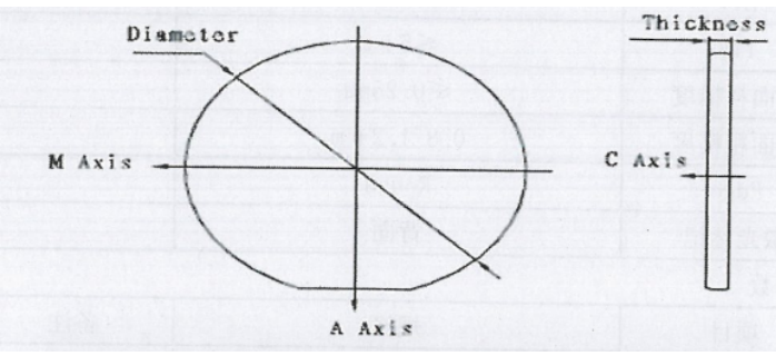
|
| Dimension | 50.80±0.10mm |
| Thickness | 430±10μm |
| Flat edge width | 16±1.0mm |
| Flat edge angle | A-plane±0.2o |
| TTV | ≤5μm |
| BOW | ≤-8~0μm |
| Front Surface Roughness | ≤0.25nm |
| Back Surface Roughness | 0.8~1.2μm |
| Edge | Round |
| Laser making | back |
About Us
We specialize in processing a variety of materials into wafers, substrates and customized optical glass parts.components widely used in electronics, optics, opto electronics and many other fields. We also have been working closely with many domestic and oversea universities, research institutions and companies, provide customized products and services for their R&D projects. It's our vision to maintaining a good relationship of cooperation with our all customers by our good reputations.
FAQ
Q: Are you trading company or manufacturer ?
We are factory.
Q: How long is your delivery time?
Generally it is 3-5 days if the goods are in stock.
or it is 7-10 days if the goods are not in stock, it is according to quantity.
Q: Do you provide samples ? is it free or extra ?
Yes, we could offer the sample for free charge but do not pay the cost of freight.
Q: What is your terms of payment ?
Payment <=5000USD, 100% in advance.
Paymen >=5000USD, 80% T/T in advance , balance before shippment.
Product Tags:

|
|
Back Surface Roughness 0.8um to 1.2um Patterned Sapphire Substrates Width 16mm Images
|